
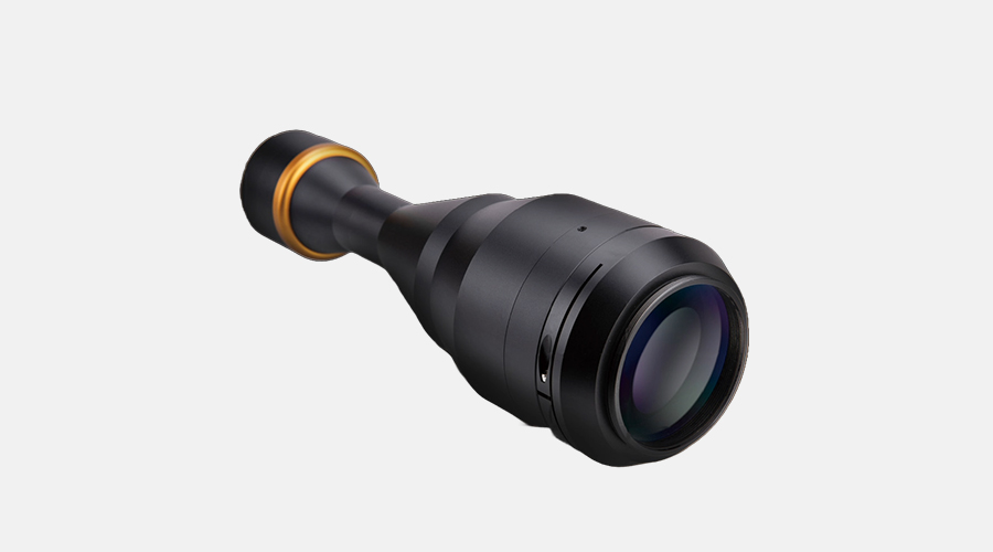
 Compatible with 7.2mm-82mm chips
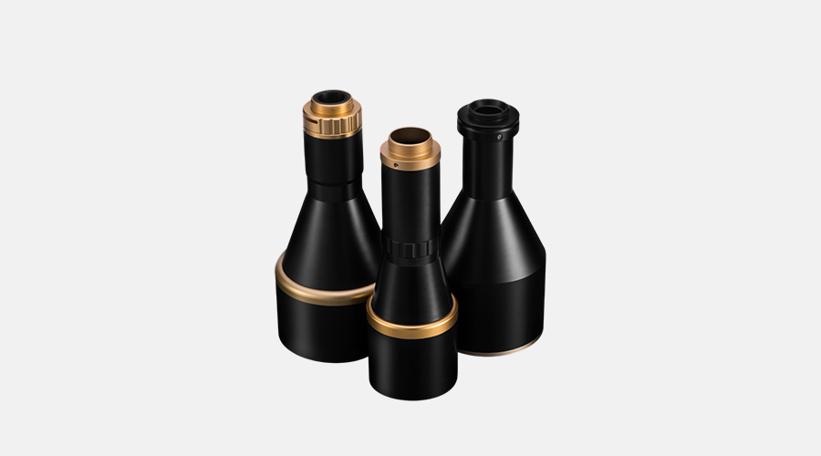 High/Low Working Distance
 Aperture telecentric lens
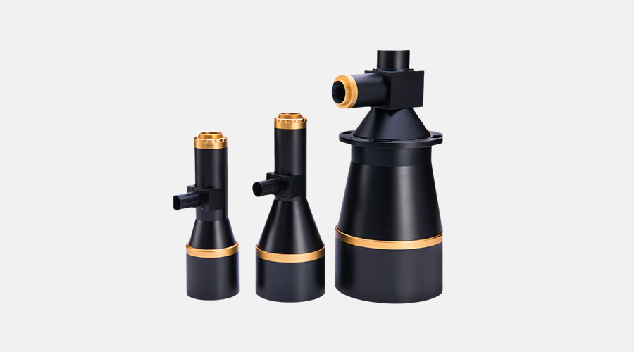 Measuring lens
 Maximum support 1.1" chips
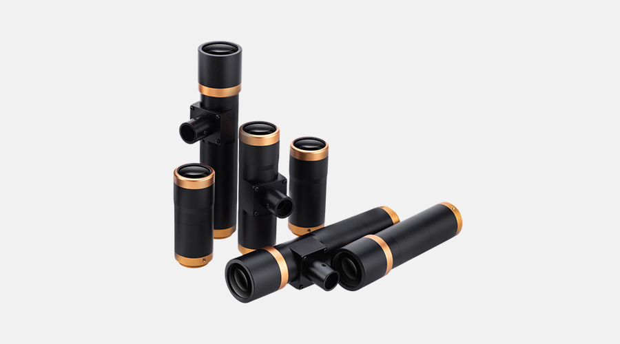 Maximum support 1.2" chips
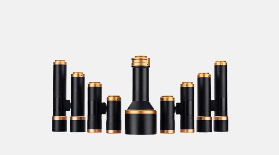 Maximum support 2/3" chips
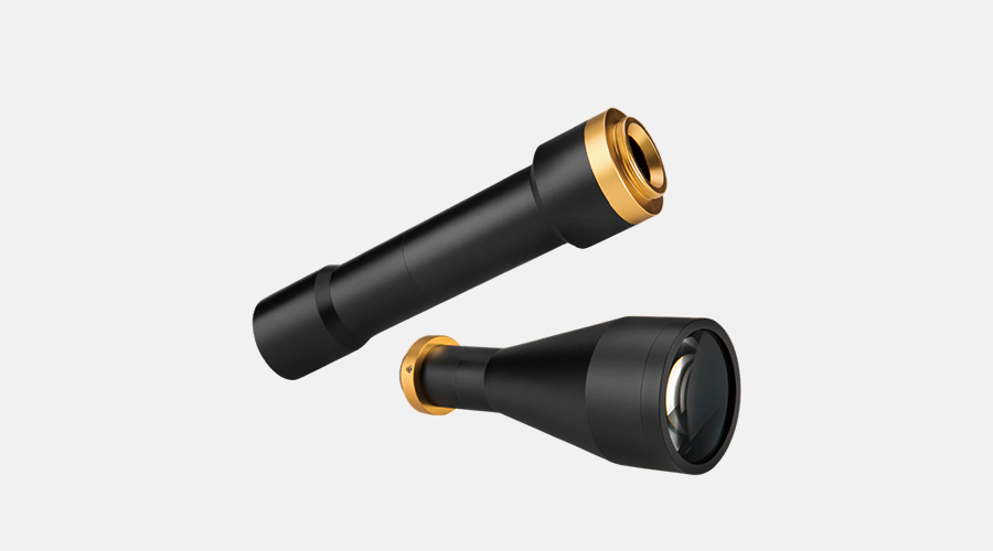 Long Working Distance
 CS mount Varifocal lens
 Varifocal board lens
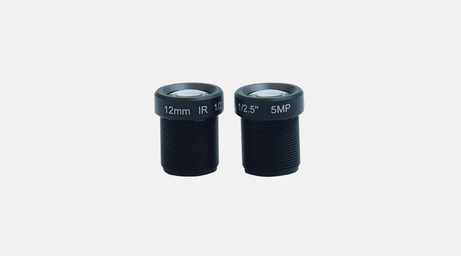 S mount lens
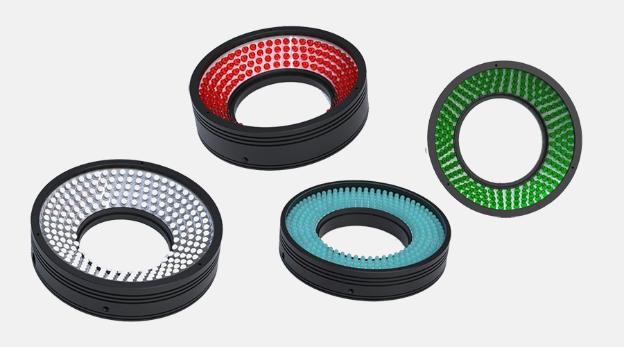 Ring light
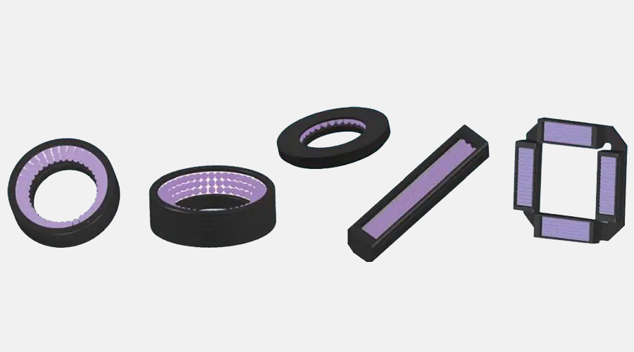 UV/IR Light
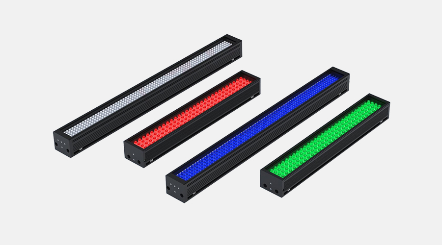 Bar light
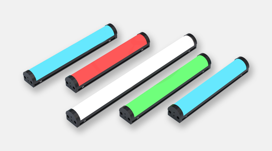 Arcuate high uniformity light
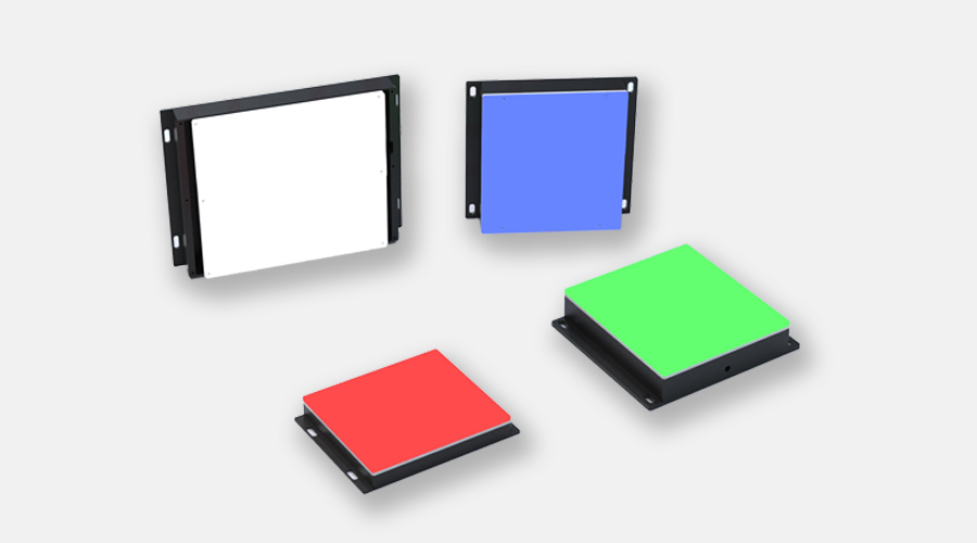 Back light
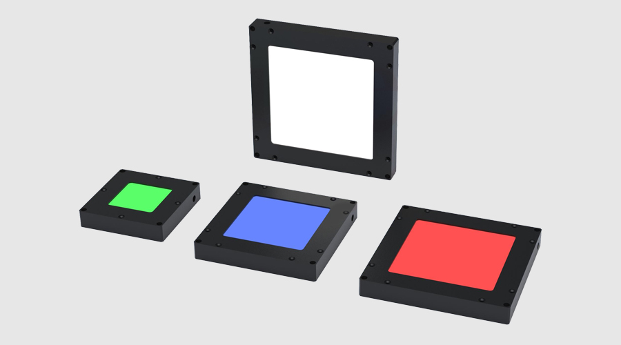 Flat light
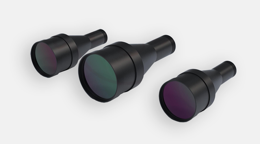 Collimated light
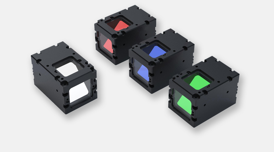 Coaxial light
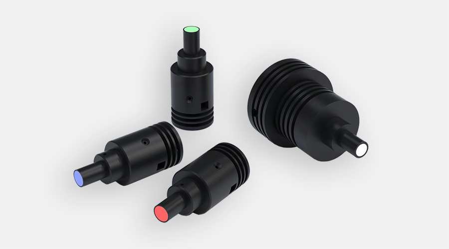 Spot light
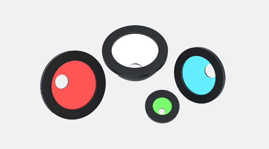 Dome light
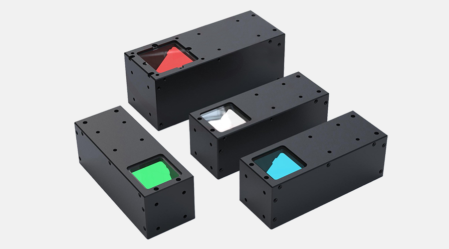 Collimated Coaxial light
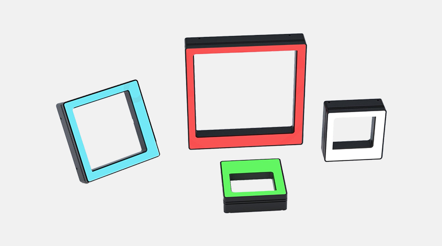 Shadowless square light
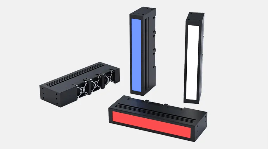 Scan light
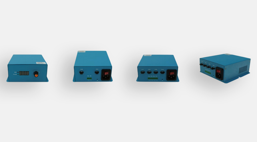 Analog controller
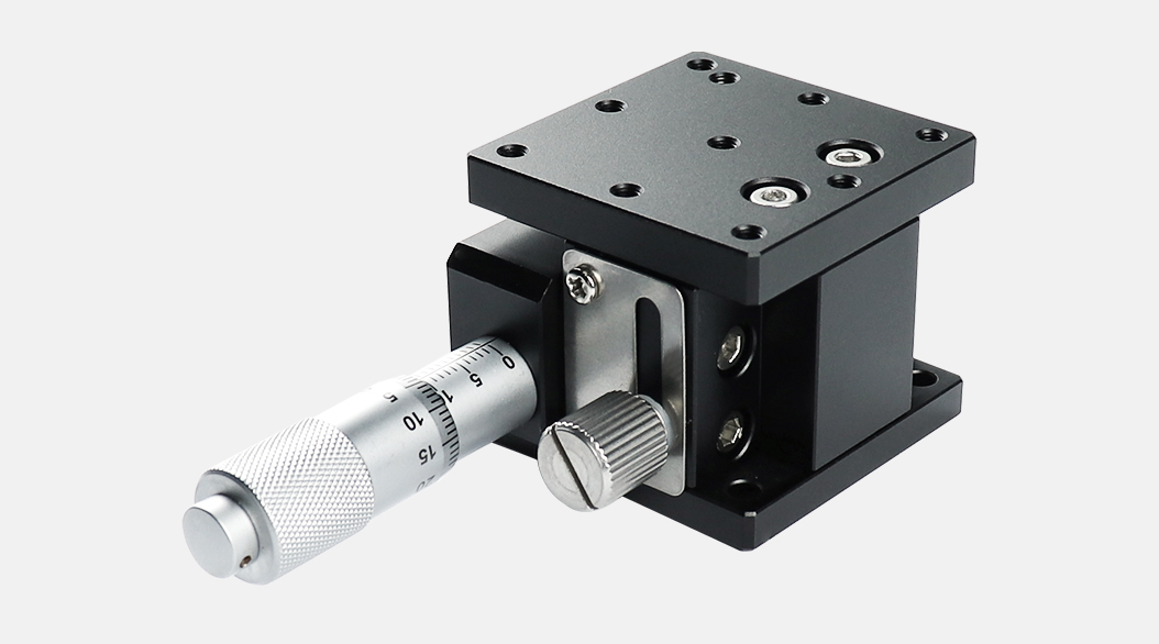 Crossed-Roller Linear guide type
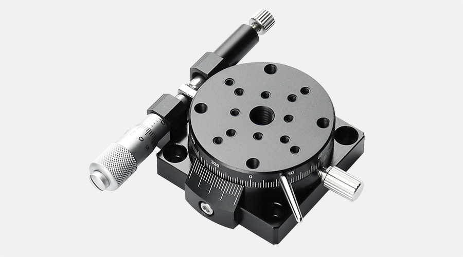 Rotary Stages XRS series
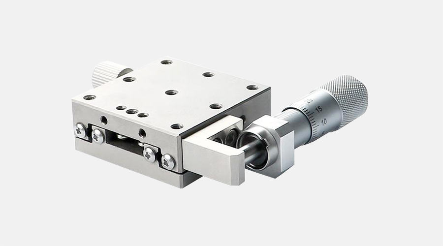 Stainless Steel Ball Bearing Linear Translation Stages
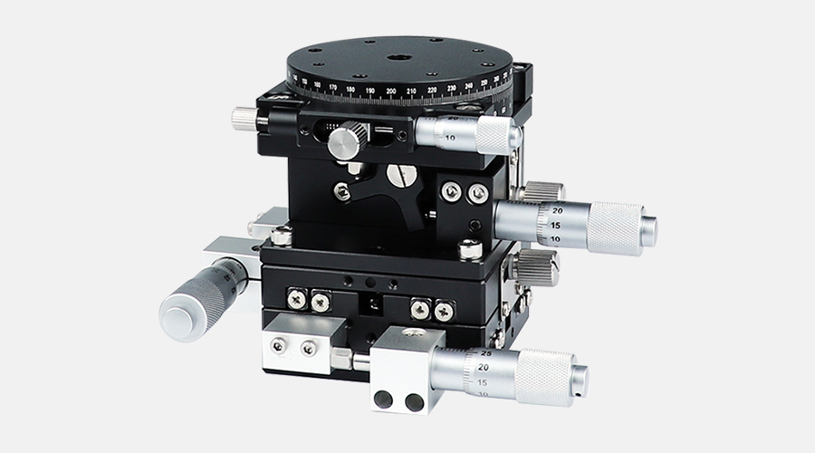 Multi-axis Translation stages
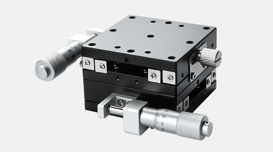 steel bar ball bearing stages
 Dovetail Type Rack&Pinion Positioning Stage
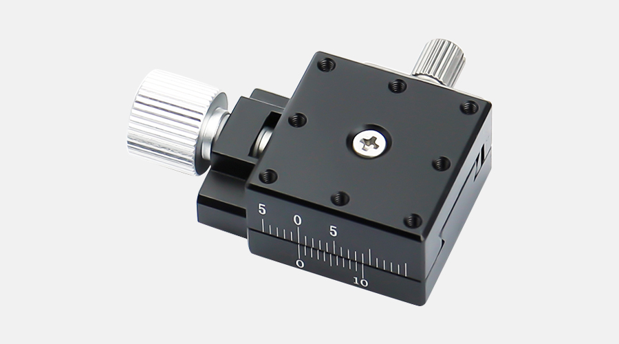 Dovetail groove high-precision screw slide


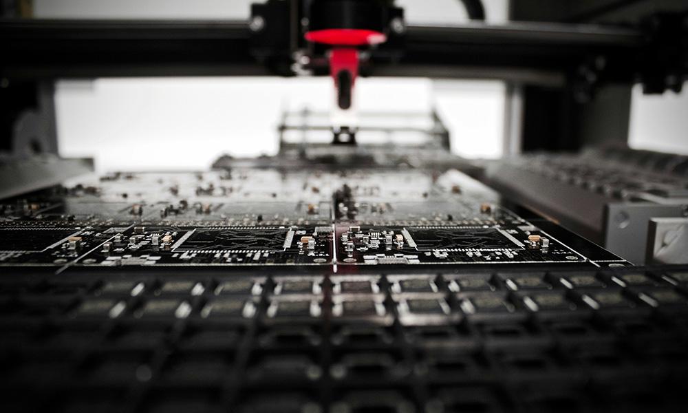
How Do Telecentric Lenses and AOI Lights Support PCB Inspection?
PCB inspection involves different types of features, so the imaging conditions cannot always be treated in the same way. Etched conductors, solder joints, component packages, and FPC alignment areas can present different shapes and surface characteristics. A Telecentric Lens can provide controlled imaging for dimensional and positional inspection, while an AOI Light can adjust illumination through different angles and colors. Combining these functions gives a machine vision system separate ways to address imaging and lighting requirements during PCB inspection.
Why Are Imaging and Lighting Both Important?
A camera can only analyze what appears in the captured image. The lens influences the geometry and detail of that image, while the light determines how the PCB surface and components are illuminated.
For PCB inspection, these two factors can have different effects. A telecentric lens may be selected when dimensional or positional information is important. An AOI light can be useful when solder joints or components require different illumination directions or colors to produce suitable image contrast.
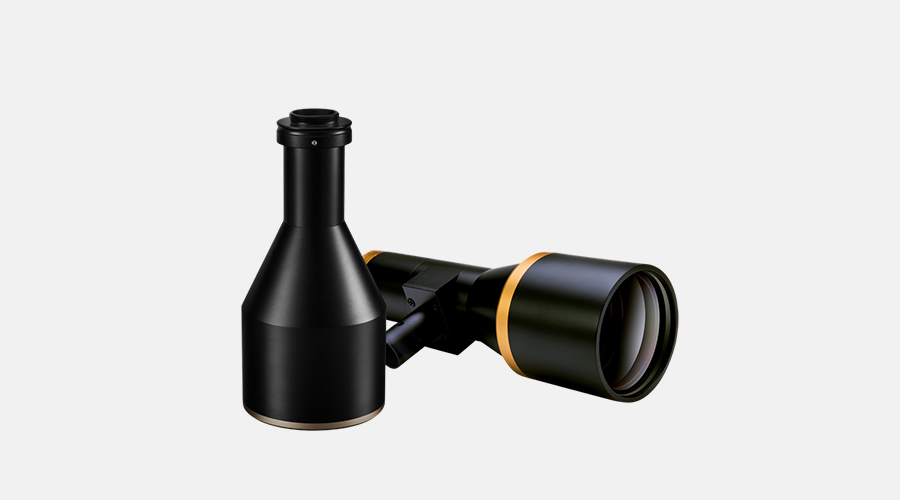
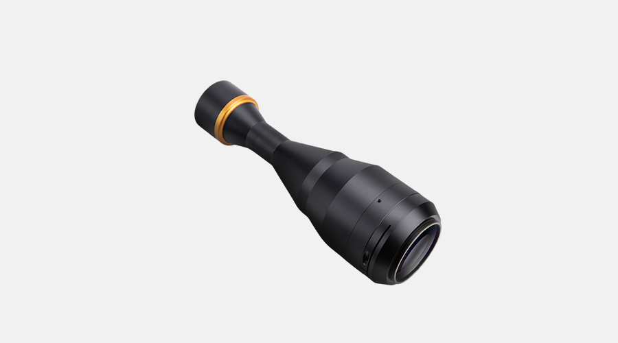
A Multi Color AOI Light can be used for PCB solder joint inspection, while the DZ Series 66mm Telecentric Lens can be used for PCB line inspection, chip package measurement, and FPC flex alignment.
The combination is therefore based on complementary functions rather than treating the lens and light as interchangeable parts.
How Does a Telecentric Lens Support PCB Inspection?
A Telecentric Lens can be considered for PCB inspection when the captured image needs controlled optical geometry. Its design can reduce perspective-related changes within its specified operating conditions, which can be useful when evaluating the dimensions or positions of PCB features.
Lens selection depends on the camera and inspection area. Sensor format, magnification, field of view, working distance, and distortion all need to correspond to the target.
The DZ Series 66mm Telecentric Lens provides one example. It has a 66 mm working distance and a customizable 0.3–10X magnification range, with support for 2/3-inch, 1/2-inch, and 1/3-inch industrial camera sensors. Its listed PCB applications include conductor nicks, shorts, and poor etching.
For these tasks, the telecentric lens is part of the imaging solution. Its suitability depends on the size of the PCB feature and the camera configuration rather than the telecentric design alone.
What Does an AOI Light Add?
An AOI Light addresses the illumination side of PCB inspection.
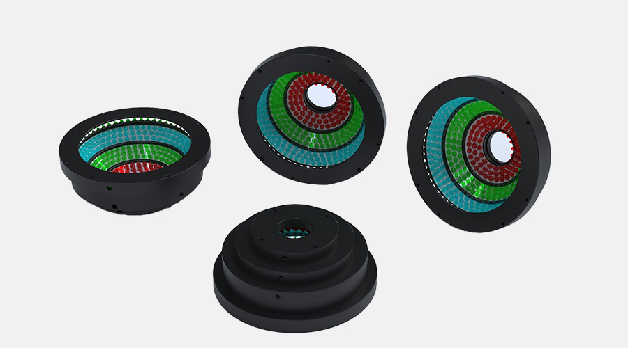
The Multi Color AOI Light for PCB Solder Joint Inspection uses a high-density LED particle array with multiple illumination angles and colors. This arrangement is relevant to PCB assemblies where components have different heights and may create shadows under illumination from one direction.
Changing the illumination angle changes how light reaches the solder joint or component surface. Different lighting zones can therefore produce different image conditions for inspection.
This is useful when surface shape or reflection affects the contrast between the target and its surroundings. Instead of relying only on higher brightness, the lighting arrangement can be adjusted around the inspection feature.
How Can Multiple Colors Assist Solder Inspection?
Color provides another variable for PCB illumination.
The AOI light uses red, blue, and white LED illumination. Different colors can produce different reflection characteristics on solder surfaces, giving the camera different image conditions.
The useful color depends on the feature being inspected and the contrast required in the captured image. A solder surface that appears with limited contrast under one illumination condition may show a different response when another color is used.
For AOI applications, this makes multi-color illumination relevant when the visual difference between solder joints, components, and surrounding PCB areas needs to be evaluated.
How Do the Two Products Work Together?
The roles of the two products can be separated clearly:
- Telecentric Lens: provides the optical imaging characteristics.
- AOI Light: provides the illumination conditions.
- Industrial Camera: captures the resulting image.
- Inspection Software: processes and evaluates the image.
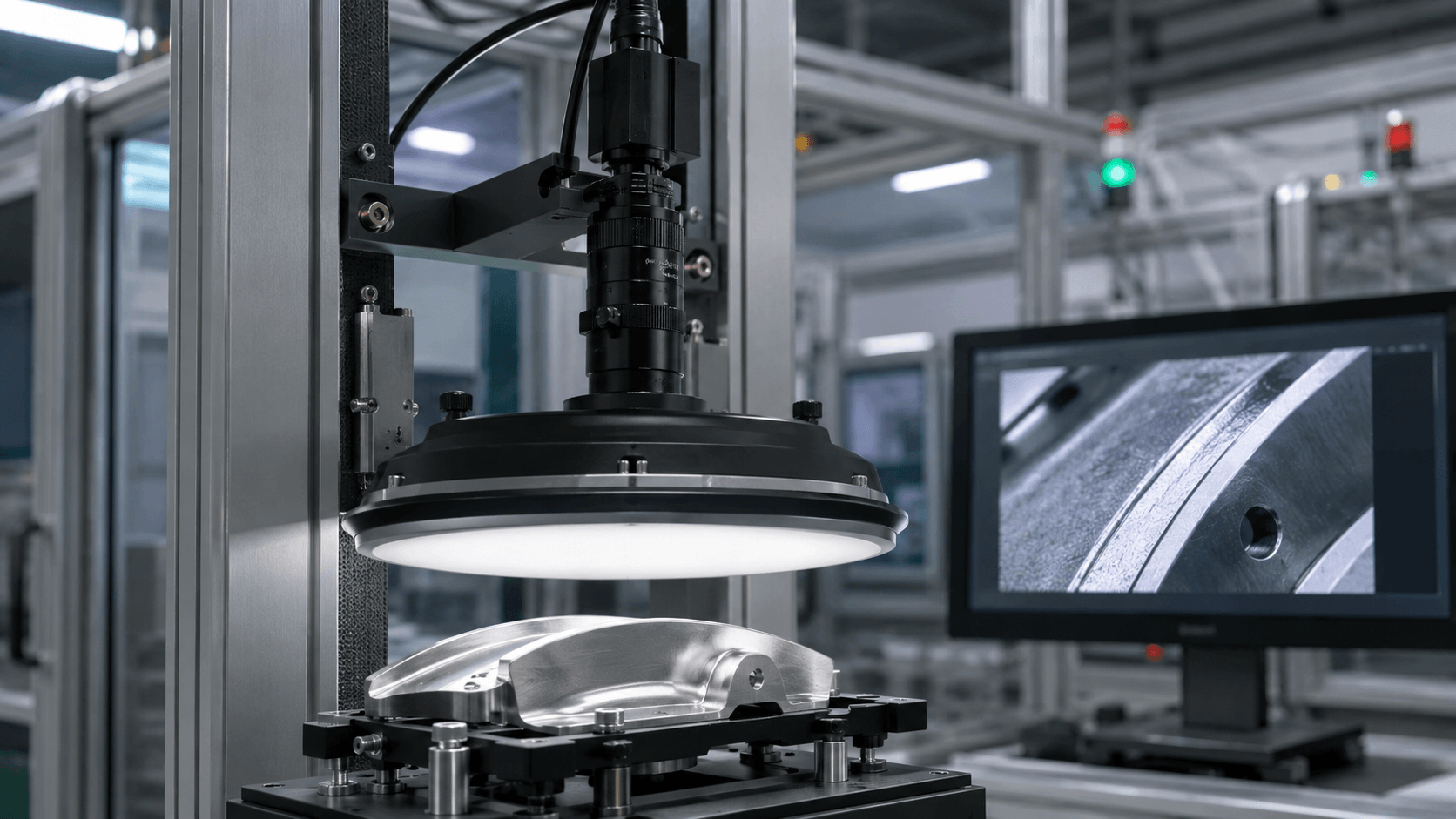
During inspection, the AOI light illuminates the PCB feature before the telecentric lens forms the image for the camera. The captured image can then be processed according to the inspection task.
For example, PCB line inspection may involve conductor nicks, shorts, or poor etching. In this case, the optical configuration needs to provide a suitable view of the circuit feature. For solder joint inspection, illumination angle and color become more important because surface shape and reflections affect the captured image.
The lens and light therefore address different stages of the same imaging process.
Which PCB Features Require Different Conditions?
PCB Lines and Etching
Conductor nicks, shorts, and poor etching are among the PCB line inspection applications listed for the DZ Series telecentric lens. These features may require attention to their position, shape, or dimensions within the captured image.
The field of view and magnification should match the size of the inspection area and the feature that needs to be analyzed.
Solder Joints
Solder joints can have curved or angled surfaces, and components surrounding the joint may affect shadows. The multi-angle capability of an AOI light can provide different illumination conditions for these areas.
Multi-color illumination adds another variable when the required contrast is difficult to obtain under a single color.
Chip Packages and FPC Alignment
The DZ Series 66mm Telecentric Lens also supports chip package measurement and FPC flex alignment. These applications place greater emphasis on the relationship between the target, camera sensor, magnification, and working distance.
The same optical setup should not automatically be applied to every PCB inspection task. The inspection feature should determine the lens and lighting requirements.
How Should the Telecentric Lens Be Selected?
For PCB inspection, lens selection should begin with the camera and target.
Sensor format determines the compatible image area.
Magnification affects the apparent size of the PCB feature.
Field of view determines how much of the board can be captured.
Working distance affects the physical arrangement around the lens.
Distortion and resolution are relevant when the image is used for dimensional or positional evaluation.
A large PCB inspection area may require a wider field of view, while a smaller feature may require greater magnification. These choices need to be considered alongside the camera sensor.
How Should the AOI Light Be Matched?
The lighting configuration should start with the inspection feature.
For solder joints and components at different heights, multiple illumination angles can provide different surface views. Multiple colors can add another contrast condition.
The physical installation also needs attention. The light should fit within the working distance and camera arrangement without interfering with the PCB or changing the intended imaging geometry.
Machine vision lighting controllers with brightness and stroboscopic control functions can also be used when the illumination conditions need adjustment within the inspection setup.
What Should Be Checked Before Integration?
Before combining a Telecentric Lens and AOI Light, identify the PCB feature that needs to be inspected and define the required image conditions.
For the lens, check:
- Camera sensor format
- Magnification
- Field of view
- Working distance
- Required image detail
For the AOI light, check:
- Illumination angle
- LED color
- Inspection area
- Component height
- Required image contrast
The camera, lens, light, and PCB also need to fit within the available installation space. Matching these factors helps keep the optical configuration focused on the actual inspection requirement.
FAQ
Why use a telecentric lens for PCB inspection?
It can provide controlled imaging for dimensional and positional inspection.
What is an AOI light used for?
It provides multi-angle and multi-color illumination for PCB inspection.
Can AOI lighting help with solder joint inspection?
A multi-color AOI light can provide different illumination conditions for solder inspection.
Why use multiple lighting angles?
Different angles can provide different views of solder joints and component surfaces.
How should the two products be matched?
Consider the PCB feature, sensor, field of view, working distance, and lighting conditions.